Solving the Materials Bottleneck in Chipmaking with HallTech's Olivier Oomen
Solving the Materials Bottleneck in Chipmaking with HallTech's Olivier Oomen
Olivier Oomen is the founder and CEO of HallTech, an Eindhoven-based company building the deposition technology needed to manufacture the next generation of semiconductors.
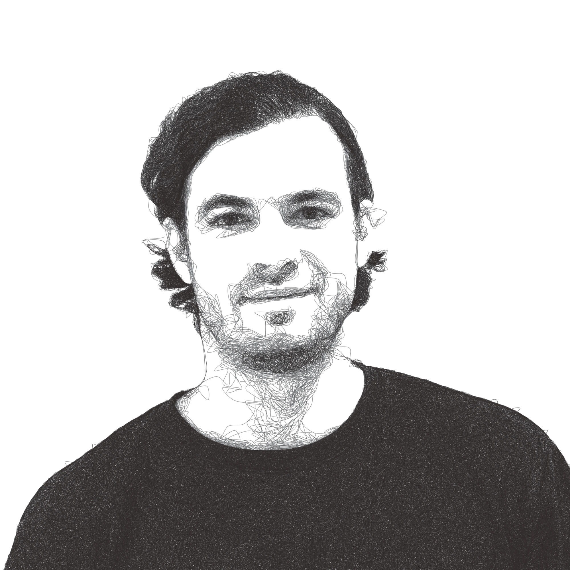
What is HallTech, and what led you to found it?
HallTech exists because of something I saw at ASML. I'm a plasma physicist by training, and I worked there for a couple of years, first in research and later in system industrialization. While I was there, I realized that lithography is no longer the bottleneck for next-generation chips. Materials are. The material stack itself is the constraint.
This drove me to start HallTech and build the process technology needed to manufacture the next generation of chips. We build unique deposition technology to make the films the industry needs next, the ones no one can produce today.
What is the problem HallTech is solving?
For 50 years this industry delivered improvements in performance per watt and performance per dollar. Now it's stuck. Moore's law is dead, and the industry can no longer rely on planar scaling to drive performance and cost improvements. The industry needs to innovate in new directions to continue scaling, and the answer is new materials.
If you look at how a chip is made, there are several process steps, but two of them really matter. One is getting the blueprint onto the chip. That is patterning, which is what ASML does, and it has become incredibly advanced. The other is depositing materials. The core of that technology is 50 years old. It has improved, sure, but nowhere near enough to deal with the dimensions now used in chip manufacturing. The nature of scaling is changing. It used to be about planar density, packing more transistors next to each other. The lithography roadmaps for that continue. But more and more, the answer is to go vertical, to go 3D. And 3D runs straight into materials.
Take 3D stacking, where you build chip layers vertically instead of spreading them out. Everyone agrees this is the next logical step in chip innovation, but the potential is hard to reach. The heat sinks and thermal layers are simply not good enough. You're pushing much more power into the chip, so you have to get the heat back out. We know exactly which materials we want. Literally no one can produce them. No one can make that molecular structure, that combination of atoms, at the thicknesses and speeds you need to get into a fab.
You see the same thing coming in optics. Everybody wants to move data with photons instead of electrons, and integrating that with modern chips is, again, a materials problem. We have ideas there too. So that's the problem. We went through the industry's roadmap for the next 15 years and looked for the pain points nobody can solve. In most cases the materials are known. Making them is the problem. That's what we're building. I said Moore's law is dead. We're going to bring it back to life.
Chip scaling is hitting a materials bottleneck rather than a lithography one. Can you walk us through that?
For the last 15 years the biggest bottleneck in scaling was going smaller. You put the lines closer to each other. That's what lithography does, it creates the patterns, and the industry got extremely good at it.
But shrinking has a side effect. The smaller everything gets, the bigger other problems become. The layers sit closer together, so they start to interact and their electrical performance degrades. At the same time, all that power concentrates in a smaller space, so the heat has nowhere to go. The transistor has kept improving. The materials have not. At some point going smaller stops being the answer.
The analogy I like to use is a Formula One car driving on a dirt road. What do you improve? Do you make the car faster, or do you fix the road? One is state of the art, which is lithography. The other is the dirt road. Going faster is the whole point of chips. So do you build a new road, or do you tune the engine? Materials are the dirt road today. Everybody keeps tuning the engine. We're building the road, so every other step can go to the next level.
The major deposition players have been at this for decades. Why is a small team in Eindhoven the one to solve the materials problem?
Material deposition has a few major players, similar to lithography. They're very good at what we call the boring layers, the routine ones that are well understood, and their platforms have been optimized for exactly those layers over 50 years. But the new materials don't need a better version of those platforms. They need a different one.
That is what we built. We went through every deposition technology out there from first principles, and we saw the fundamental flaws in each of them. So we reasoned from the bottom up. If you want these films, what does the machine have to look like? We started from the specs the industry needs and designed backward from there. What came out is a fundamentally new way of depositing materials. It is fast, high quality, and low temperature, with real control over the energy of the atoms as they land and the structure they form. That is exactly what is missing today.
Eindhoven, in the Brainport region, probably has the highest density of top plasma physics and high-precision engineering expertise in the world, thanks to the ecosystem around ASML. A small team, the right people, and the ability to move fast. In my view that's exactly what this problem needed.
Those are big claims for a young company. What have you actually shown so far, and where will your technology show up first?
Fair question. Our proof-of-concept source is running in Eindhoven today. The first films that came off it went to external labs, and the quality is on par with the best tools in the industry. From the very first films, and at low temperature. That last part matters. Low temperature is exactly what advanced chip stacks demand, and it is exactly where existing tools lose their quality. We got both at once.
The first application is heat. That 3D stacking problem I mentioned, where power density goes up while the thermal materials to get it back out don't exist. Those films are our first target. After that come insulating layers tuned for optical performance and then potentially conducting films. Same platform, new films every time.
Europe holds a lot of semiconductor IP but a relatively small share of the market. Can you scale in Europe, or do you have to look elsewhere?
For part of the journey, absolutely. Europe is uniquely positioned for what I call zero to one, because we have so much knowledge and IP. For building a genuinely new semiconductor technology, Europe is miles ahead of any other part of the world. That phase happens here in Eindhoven, and there's no better place for it.
Scaling that into an industry-defining company has more challenges here. Maybe it's mindset. Probably it's regulation, and quite possibly it's funding, or risk appetite. We all know the arguments, and they're probably all true to some extent. What Europe has is talent: very skilled, very precise scientists and engineers. What the U.S. has is freedom, speed, and the room to fail. Neither side has the full package. So for us it's not either-or. We focus on scaling the company as fast as we can. We're also weighing the best strategy and locations to do that.
What about Asia? Do you see European deep tech moving in that direction, or is the pull still primarily toward the U.S.?
Asia is the leader in chip manufacturing today. Look at where some of the strongest semiconductor companies sit: TSMC, Samsung, Tokyo Electron. So of course we focus on Asia. Everyone serious does, because that's where the fabs are. But that is a commercial decision. Whether European deep tech should move there is a different matter. The customers are in Asia. The capital and the scaling speed are in the U.S. And new technology is born here in Europe. Those things don't all have to happen in the same place.
What I do see is countries and regions insourcing more and more of their own development. The U.S. is the obvious example. Over the next couple of years, the industry will spend more than $500 billion purely on building new fabs and new production lines. That was not really a focus before. And each region builds for its own priorities. The U.S. right now is extremely focused on data centers and high-power chips for compute. Parts of Asia may lean more toward automotive and robotics. Semiconductor manufacturing is accelerating everywhere, and the need is both technological and geopolitical.
Countries are starting to realize that the future of humanity is directly correlated with the future of compute. It's an almost cyberpunk future. Compute will be the new oil. There's a huge shift in power underway. People are fighting for the resources behind the technology that makes the difference. That will only accelerate over the next 10 years. We're at the start of a new gold rush, but for chips.
How do you define deep tech?
For me, deep tech is innovation that's heavy on IP and pushes the boundaries of physics. Because of my background that mainly means hardware. It also means doing something nobody has achieved before. And it means years of investment before you see any revenue.
I'd say 80% of it is hardware. The other 20% is something like AI. Large language models are an amazing example. The models from companies like Anthropic and OpenAI count 100% as deep tech. A lot of IP, a lot of know-how, and really pushing physical limits. But think about where those limits actually sit. Every model is limited by compute. Compute is limited by chips. And chips, at this point, are limited by materials. So deep tech runs on deep tech. And that's where we build.

Infinite Frontiers is made possible by HAUS, the leading public relations agency for deep tech startups and scaleups